- 您现在的位置:买卖IC网 > Sheet目录3876 > PIC16F639-E/SS (Microchip Technology)IC MCU FLASH 2KX14 20SSOP
Micrel, Inc.
KSZ8841-PMQL
October 2007
33
M9999-100407-1.5
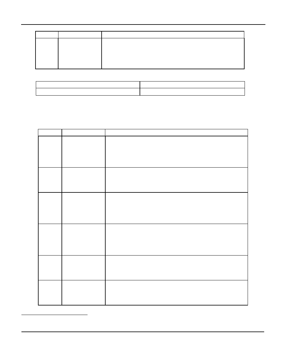
Bit
Default
Description
Provides interrupt line routing information. The basic input/output system
(BIOS) writes the routing information into to this field when it initialized and
configures the system. The value in this field indicates which input of the
system interrupt controller is connected to the K8841P’s interrupt pin. The
driver can use this information to determine priority and vector information.
Values in this field are system architecture specific.
The following table shows the access rules of the register.
Category
Description
Value after hardware reset
0x281401XX
Capabilities ID Register (CCID Offset 50H)
The CCID register is a read-only register that provides information on the KSZ8841-PMQL power management
capabilities. The following table shows the CCID register bit fields. The CCID register bits [31-16] are mirrored with
PMCR register bits [15-0].
Bit
Default
Description
31
0
PME Support D3 (cold)
If this bit is set, the KSZ8841-PMQL asserts PME in D3(cold) power state.
Otherwise,
the KSZ8841-PMQL does not assert PME in D3(cold).
The value of this bit is loaded from the PME_D3_cold bit in the EEPROM.
30
1
PME Support D3 (hot)
The value of this bit is 1, indicating that the KSZ8841-PMQL may assert
PME in
D3(hot) power state.
29
0
PME Support D2
If this bit is set, the KSZ8841-PMQL asserts PME in D2 power state.
Otherwise, the
KSZ8841-PMQL does not assert PME in D2 state.
The value of this bit is loaded from the PME_D2 bit in the EEPROM.
28
0
PME Support D1
If this bit is set, the KSZ8841-PMQL asserts PME in D1 power state.
Otherwise, the
KSZ8841-PMQL does not assert PME in D1 state.
The value of this bit loaded from the PME_D1 bit in the EEPROM.
27
0
PME Support D0
1
The value of this bit is 0, indicating that the KSZ8841-PMQL does not
assert PME in
D0 power state.
26
0
D2 Support
If this bit is set, it indicates that the KSZ8841-PMQL support D2 power
state.
The value of this bit is loaded from the D2_SUP bit in the EEPROM.
1 References to D0, D1, D2, and D3 are power management states defined in a similar fashion to the way they are defined for PCI.
For more information, refer to the PCI specification at www.pcisig.com/specifications/conventional/pcipm1.2.pdf.
发布紧急采购,3分钟左右您将得到回复。
相关PDF资料
PIC18LF24K22-I/SS
IC PIC MCU 16KB FLASH 28SSOP
PIC24F08KL402-I/ML
IC MCU 16BIT 8KB FLASH 28-QFN
PIC24F08KL302-I/SP
IC MCU 16BIT 8KB FLASH 28-SPDIP
PIC16LF1938-I/ML
IC MCU 8BIT FLASH 28QFN
PIC24F08KL402-I/MQ
IC MCU 16BIT 8KB FLASH 28-QFN
PIC16LF1938-I/MV
IC MCU 8BIT 28KB FLASH 28UQFN
PIC18F24K22-I/SS
IC PIC MCU 16KB FLASH 28SSOP
PIC16F1938-I/ML
IC MCU 8BIT FLASH 28QFN
相关代理商/技术参数
PIC16F639-I/P
功能描述:8位微控制器 -MCU 4kb 128 RAM 12 I/O RoHS:否 制造商:Silicon Labs 核心:8051 处理器系列:C8051F39x 数据总线宽度:8 bit 最大时钟频率:50 MHz 程序存储器大小:16 KB 数据 RAM 大小:1 KB 片上 ADC:Yes 工作电源电压:1.8 V to 3.6 V 工作温度范围:- 40 C to + 105 C 封装 / 箱体:QFN-20 安装风格:SMD/SMT
PIC16F639-I/SO
功能描述:8位微控制器 -MCU 4kb 128 RAM 12 I/O RoHS:否 制造商:Silicon Labs 核心:8051 处理器系列:C8051F39x 数据总线宽度:8 bit 最大时钟频率:50 MHz 程序存储器大小:16 KB 数据 RAM 大小:1 KB 片上 ADC:Yes 工作电源电压:1.8 V to 3.6 V 工作温度范围:- 40 C to + 105 C 封装 / 箱体:QFN-20 安装风格:SMD/SMT
PIC16F639-I/SS
功能描述:8位微控制器 -MCU 4kb 128 RAM 12 I/O RoHS:否 制造商:Silicon Labs 核心:8051 处理器系列:C8051F39x 数据总线宽度:8 bit 最大时钟频率:50 MHz 程序存储器大小:16 KB 数据 RAM 大小:1 KB 片上 ADC:Yes 工作电源电压:1.8 V to 3.6 V 工作温度范围:- 40 C to + 105 C 封装 / 箱体:QFN-20 安装风格:SMD/SMT
PIC16F639-I/SS
制造商:Microchip Technology Inc 功能描述:8-Bit Microcontroller IC
PIC16F639T-I/SO
功能描述:8位微控制器 -MCU 4kb 128 RAM 12 I/O RoHS:否 制造商:Silicon Labs 核心:8051 处理器系列:C8051F39x 数据总线宽度:8 bit 最大时钟频率:50 MHz 程序存储器大小:16 KB 数据 RAM 大小:1 KB 片上 ADC:Yes 工作电源电压:1.8 V to 3.6 V 工作温度范围:- 40 C to + 105 C 封装 / 箱体:QFN-20 安装风格:SMD/SMT
PIC16F639T-I/SS
功能描述:8位微控制器 -MCU 4kb 128 RAM 12 I/O RoHS:否 制造商:Silicon Labs 核心:8051 处理器系列:C8051F39x 数据总线宽度:8 bit 最大时钟频率:50 MHz 程序存储器大小:16 KB 数据 RAM 大小:1 KB 片上 ADC:Yes 工作电源电压:1.8 V to 3.6 V 工作温度范围:- 40 C to + 105 C 封装 / 箱体:QFN-20 安装风格:SMD/SMT
PIC16F648A-E/ML
功能描述:8位微控制器 -MCU 7KB 256 RAM 16 I/O RoHS:否 制造商:Silicon Labs 核心:8051 处理器系列:C8051F39x 数据总线宽度:8 bit 最大时钟频率:50 MHz 程序存储器大小:16 KB 数据 RAM 大小:1 KB 片上 ADC:Yes 工作电源电压:1.8 V to 3.6 V 工作温度范围:- 40 C to + 105 C 封装 / 箱体:QFN-20 安装风格:SMD/SMT
PIC16F648A-E/P
功能描述:8位微控制器 -MCU 7KB 256 RAM 16 I/O RoHS:否 制造商:Silicon Labs 核心:8051 处理器系列:C8051F39x 数据总线宽度:8 bit 最大时钟频率:50 MHz 程序存储器大小:16 KB 数据 RAM 大小:1 KB 片上 ADC:Yes 工作电源电压:1.8 V to 3.6 V 工作温度范围:- 40 C to + 105 C 封装 / 箱体:QFN-20 安装风格:SMD/SMT